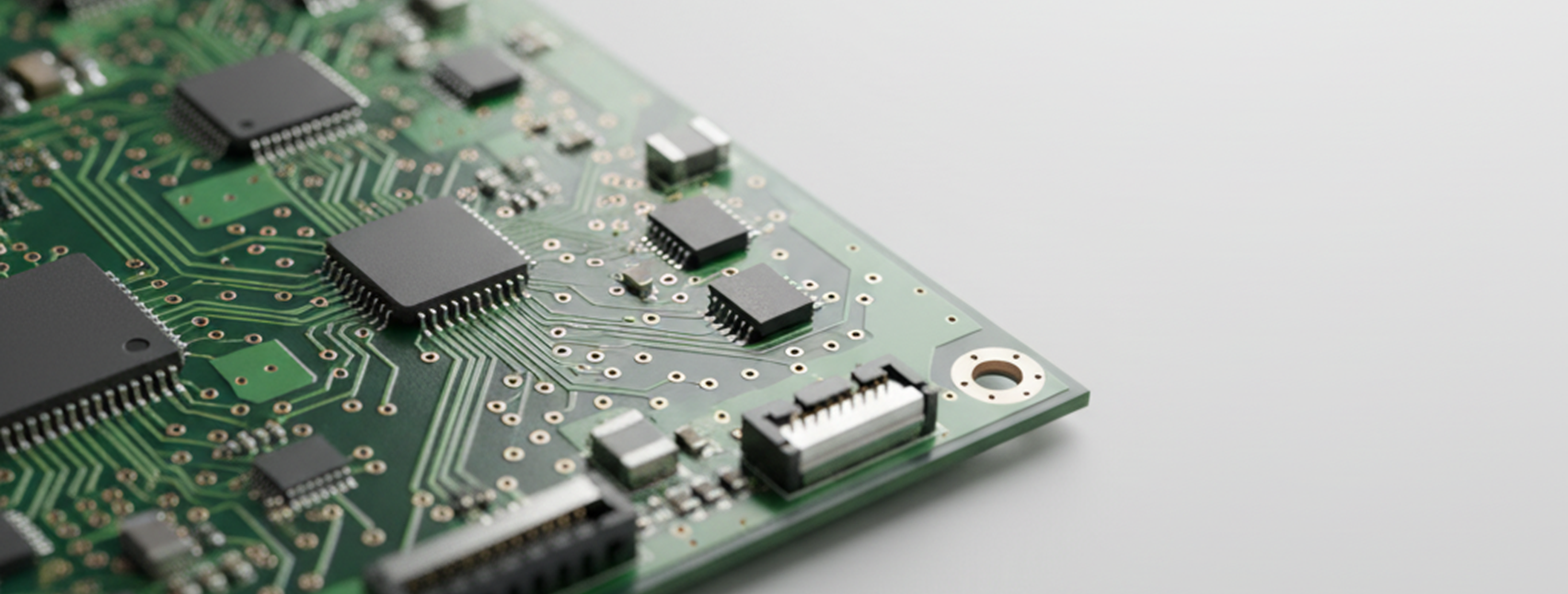
PCB ARTWORK
Perfect Circuits Start with Perfect Artwork.
From design to Circuit
We prepare your PCB artwork so it’s accurate and ready for production from the start.
This helps your design move into real circuits smoothly, reduces production issues, and supports faster, more reliable output for your business.
Our Capability, over 10 years of experience
We precision in every layer.
185
Projects / year
200
Companies
Rigid, Fex, Rigid-flex
Board type
NTH, TH, HDI
Via Type
")
Capability Statement
Maximum size up to 500*375 mm.
Stack up design
- Fill-Stack Vias
- Build-up Vias
- Throught-Hole Vias
Pin
≈ 17,195 pins
Pin – pair
≈ 11,887 nets
Nets
≈ 4,143 nets
Layer
≈ 1-40 layers
Size
≈ 500x375mm
Size
≈ 500x375mm
Product Design

Rigid

Flex

Rigid-Flex
Service & Solution

New / Modify Artwork

FP Library Creation

Panel Creation

Creation

PCB Simulation

Schematic Capture / Gerber to Artwork
Application Apply

Automotive

Medical

Consumer

Sensor

Telecommunication
Providing high-standard
to support your success.
Japan-Standard Workflow
Designs crafted to meet Japanese industrial standards.
Multi-Industry Expertise
Proven experience delivering solutions across diverse industries.
Client-Focused Flexibility
Adaptive designs tailored to each client’s unique needs.